Huawei wants better chips, so it is building upward
In brief
Huawei is improving its Kirin chips by distributing circuits across vertically connected layers, an approach it calls LogicFolding, instead of relying only on shrinking transistors. Its own paper claims 53.5% higher transistor density and 41% lower power draw at equal performance than the Kirin 9030 Pro. The first shipping chip of this generation, the Kirin 9050 Pro, beats two older mid-range rivals in a single Geekbench run, but public data cannot yet isolate what LogicFolding contributes.
When shrinking a chip's components gets hard, there is another option left: change where you put them. Huawei is betting on spreading its circuits across several layers to bring them closer together.1
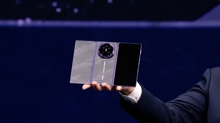
The company already lists the Kirin 9050 Pro on the official spec sheet for its Mate XT 2. Behind the Kirin family sits HiSilicon, Huawei's chip design arm, which contracts the manufacturing out to third parties.2,3
Two separate jobs are worth pulling apart here. HiSilicon designs the chips; the Dutch company ASML builds the lithography machines that make their minuscule components possible. US and Dutch export controls restrict access to certain advanced ASML equipment and complicate Huawei's manufacturing chain.3,4,5
For decades, one of the main ways to improve a processor has been to shrink the size of its components. The smaller they are, the more transistors fit in the same area. But there is another way to get more out of that space: build upward.6,7
Picture two circuits, A and B, two millimetres apart inside a chip. It sounds like a tiny distance, but pushing signals along the wiring between them costs time and energy. If the design allows B to sit on top of A, a vertical connection can shorten the trip. The two millimetres are there to illustrate the idea — they are not a published Kirin measurement.1,7
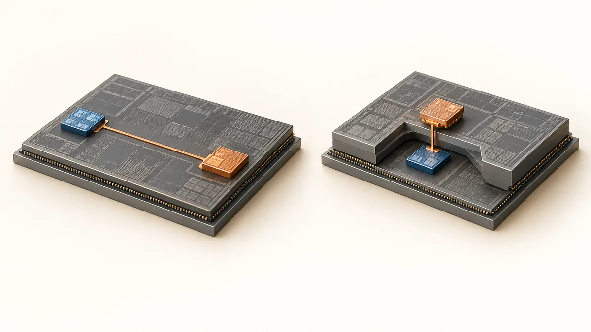
Huawei calls its approach LogicFolding. It does not physically fold the chip: it distributes circuits across layers that are connected vertically. The first implementation concentrates on the paths that cap the processor's speed.1
The metaphor comes with a caveat: conventional chips already contain plenty of layers of materials and wiring. What changes is how the active circuits are distributed and how they connect to each other.1,8
In its paper, Huawei claims that the design it calls Kirin 2026 increases transistor density by 53.5% over the Kirin 9030 Pro. It also reports 41% lower power draw when compared at equal performance. These are figures published by the company itself, and they do not translate into the same percentage gain across every application.1
So what do the benchmarks show? A Geekbench entry uploaded on 7 September 2026 gives the following scores for a device identified as HUAWEI LAP-AL10. Two familiar processors help put the result in context:
| Device or processor | Geekbench 6: single-core | Geekbench 6: multi-core | Reference |
|---|---|---|---|
| HUAWEI LAP-AL10 — Kirin, model unspecified | 1464 | 5037 | 9 |
| Snapdragon 870 | 1298 | 3520 | 10 |
| Dimensity 1000+ | 1031 | 3123 | 11 |
The Huawei entry identifies the processor only as "hisilicon kirin": it does not confirm that this is a Kirin 9050 Pro. It is also a single run, whereas the other figures come from NanoReview's aggregated results.9,10,11
The score beats both reference points in the table, but it still is not enough to measure what LogicFolding contributes, or to crown the 9050 Pro the most powerful chip in its class.
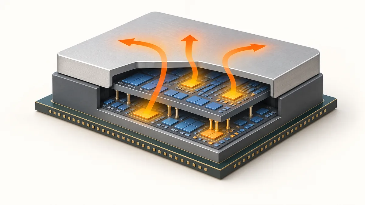
Building upward brings its own difficulties. Stacking components that generate heat can make them harder to cool, so making better use of the space means balancing performance, power draw and temperature. It is a well-known challenge in 3D integration, and one that organisations such as Imec are researching too.12
Huawei expects to extend the folding to more circuits and more layers in future generations. The approach opens up a way to improve its processors without relying solely on making their components smaller. How much ground it closes on its rivals will have to be judged from tests of shipping products.1
Sources
- He Tingbo, Huawei. A time scaling theory for multi-layer electronic systems. Section 4: LogicFolding and the Kirin 2026 results; table 2: the roadmap.
- Huawei. Official Mate XT 2 spec sheet. Confirms that it carries the Kirin 9050 Pro.
- Huawei. Description of HiSilicon as a fabless chip design company.
- ASML. Statement on the Dutch export controls.
- ASML. Statement on the partial revocation of licences and the US restrictions.
- ASML. Microchip basics. Miniaturisation and transistor density.
- Imec. 3D integration of circuits. Stacking and shorter connections.
- ASML. How microchips are made. Structure and multiple layers.
- Geekbench Browser. HUAWEI LAP-AL10 entry. Geekbench 6.7.1; content consulted via the transcript provided.
- NanoReview. Snapdragon 870: aggregated results. Secondary source.
- NanoReview. Dimensity 1000+: aggregated results. Secondary source.
- Imec. Thermal challenges of 3D stacking.
Quick answers
- What is Huawei's LogicFolding?
- A chip design approach that spreads active circuits across several layers connected vertically, so signals between them travel shorter paths. It does not physically fold the chip, and it does not depend on manufacturing smaller transistors.
- Which Huawei chip uses LogicFolding?
- Huawei's paper reports figures for a design it calls Kirin 2026, compared against the Kirin 9030 Pro. The Kirin 9050 Pro, listed on the Mate XT 2's official spec sheet, is the first commercial chip of that generation.
- Is the Kirin 9050 Pro faster than rival processors?
- Not proven yet. One Geekbench 6 run of a device identified as HUAWEI LAP-AL10 scored 1464 single-core and 5037 multi-core, above a Snapdragon 870 and a Dimensity 1000+, but the entry does not confirm the exact chip and a single run cannot rank it against current flagships.
- What is the main drawback of stacking circuits?
- Heat. Components that generate heat are harder to cool when stacked, so any gain in density has to be balanced against power draw and temperature. It is a known challenge of 3D integration that research centres such as Imec are working on.